
Original briefings. Zero spin.
Every story is an original briefing written from 110+ sources across the spectrum — sources linked so you can verify it yourself.
 economy
Notable (6/10)
August 27, 2026 at 07:18 PM
economy
Notable (6/10)
August 27, 2026 at 07:18 PM
SK Hynix Breaks Ground on $4 Billion Indiana Plant, but Mass Production Is Still Three Years Out
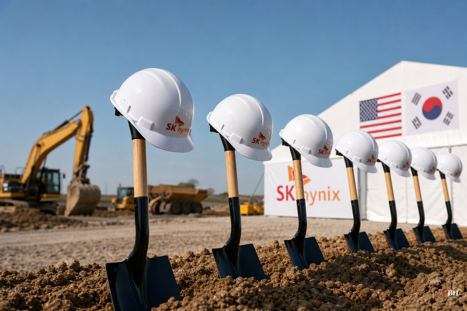
SK Hynix broke ground Thursday on its first U.S. manufacturing facility, a $4 billion advanced packaging plant in West Lafayette, Indiana, on land owned by Purdue University. CEO Kwak Noh-Jung says the site will make Indiana a "key HBM production base in America" by 2030.
This isn't a chip fab. It's a packaging plant. DRAM wafers will still be manufactured in South Korea and China, according to CNBC. They'll be shipped to Indiana to be stacked and packaged into high-bandwidth memory, or HBM, the specialized chips that power Nvidia's AI accelerators. The cleanroom where that packaging happens won't even open until October 2028, according to Kwak's own remarks reported by the Korea Herald. Mass production of next-generation HBM4E doesn't start until the third quarter of 2029, per BigGo Finance and mbiz.heraldcorp.
That's a three-year runway before this thing produces a single commercial chip.
The taxpayer angle
The project is getting help from Washington. Under the CHIPS and Science Act, SK Hynix could receive up to $458 million in direct funding and $500 million in loans, according to Crypto Briefing and the Korea Herald. That's nearly a billion dollars in federal support for a facility that employs roughly 1,000 people directly, with about 7,000 total jobs counting construction and indirect employment, per Crypto Briefing.
Commerce Department official Bill Frauenhofer said the project "represent[s] an important opportunity not only to bring cutting-edge capabilities to the United States," according to the Korea Herald. Indiana Governor Mike Braun called it the "biggest development project in Indiana's history," and Republican Senator Todd Young said it addresses how the U.S. "designed many of the world's most advanced chips, while allowing too much of the manufacturing ecosystem to migrate overseas," according to CNBC.
Fair point from Young. The U.S. does need more of the chip supply chain onshore. But packaging is the tail end of that chain, not the front end. Commerce Secretary Howard Lutnick made that exact distinction in July, publicly calling on SK Hynix and Samsung to build actual front-end chip fabs in the U.S., not just packaging plants, according to CNBC. Kwak's response Thursday was noncommittal. SK Hynix is "open to every site or every country," he said, but nothing is decided.
The money is real, the demand is real
Whatever the politics, the business case is not fake. SK Hynix posted revenue just under $65 billion in 2025, with profit roughly doubling to $28 billion, according to Breitbart. The company's market cap is up roughly sevenfold over the past year, topping $1 trillion, per CNBC. SK Hynix listed American depositary receipts on the Nasdaq in July, raising $26.5 billion, the largest U.S. share sale ever by a foreign company, according to both CNBC and Breitbart.
Demand for HBM is genuinely outstripping supply. Apple raised prices on Macs and iPads this year because of memory chip cost increases, according to Breitbart. South Korean union workers at SK Hynix are set to receive average compensation packages of $547,000 this year, driven by the memory price surge, according to Fox News.
Kwak told reporters after Thursday's ceremony that he sees "no clear signals foreshadowing a downturn" and expects the AI-driven memory boom to run through the end of 2030, according to BigGo Finance. He argues HBM is different from past memory cycles because customers and manufacturers co-design the product, making demand more predictable than the commodity boom-bust cycles of old. Kwak is the CEO of the company selling the chips, so his optimism comes with an obvious incentive to talk up the cycle.
Europe had a nearly identical opportunity and blew it
Intel had approved a €4.6 billion assembly and testing plant near Wroclaw, Poland, promising 2,000 jobs. The European Commission approved €1.7 billion in Polish state aid in September 2024. Intel suspended the project that same month and canceled it outright in July 2025, according to The Next Web.
The EU's own Court of Auditors projected the bloc will hit just 11.7% of global chip production value by 2030, against a stated target of 20%, per The Next Web's reporting on the auditors' findings. Total EU chip funding through 2030 sits around €86 billion, versus roughly €405 billion spent by the largest global chipmakers in just three years.
SK Hynix Vice Chairman Yu Jeong-joon said the company's total U.S. investments across semiconductors, energy and advanced technology are expected to exceed $45 billion by 2030, according to the Korea Herald. Whether any of that includes an actual front-end fab, the kind Lutnick wants, remains an open question. Kwak said Thursday the company is still shopping for the right site.
Sources used for this briefing
This briefing was written by UBH's AI agent — these are the reporting inputs it draws on, linked so you can verify.