
Unbiased headlines. Facts, not spin.
Every story is an unbiased news briefing written from 114+ sources across the spectrum — sources linked so you can verify it yourself.
 tech
Major Story (7/10)
October 14, 2026 at 12:59 AM
tech
Major Story (7/10)
October 14, 2026 at 12:59 AM
Applied Materials Opens $5 Billion EPIC Chip R&D Center in Sunnyvale With TSMC, Intel, Samsung
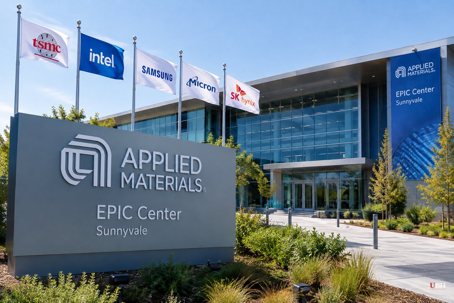
Applied Materials opened the largest building in its corner of Silicon Valley on Monday, Oct. 12. The EPIC Center, short for Equipment and Process Innovation and Commercialization, sits on the company's Sunnyvale, California campus.
The company calls it the world's largest facility dedicated to collaborative semiconductor process technology and manufacturing equipment R&D. Applied says total capital investment is expected to reach $5 billion.
What got built
The structure covers 600,000 square feet and holds nearly four acres of cleanroom space. Construction took more than six million labor hours over roughly two years.
Applied's numbers for the build: enough concrete to fill 34 Olympic-sized swimming pools and enough steel for two Eiffel Towers. Thirty-four roof trusses cover the cleanrooms, each nearly 300 feet long.
Silicon Valley has plenty of chip companies and few chip factories. Most semiconductor facilities now operate overseas or in other states. A project of this size in Sunnyvale is a rare physical bet on domestic chip R&D.
Rivals under one roof
The founding partners are TSMC, Intel, Samsung Electronics, Micron and SK hynix. Broadcom, Advantest, SCREEN, KIOXIA and Besi are innovation partners. Research partners are Arizona State University, Rensselaer Polytechnic Institute, Stanford, UC Berkeley and UCLA's Samueli School of Engineering.
Several of these companies compete head to head. Micron and SK hynix, both memory makers, will each have private test facilities inside the building, packed with advanced equipment and staffed alongside dedicated Applied teams.
Each partner will station researchers on site and get early access to Applied's newest tools. The work targets chips three to four generations ahead of what is in production today. "We're working four generations ahead of time," CEO Gary Dickerson told EE Times before the opening. "Whoever brings those innovations to market fastest is going to win."
The pitch: kill the handoffs
Applied's argument is about how chip R&D is organized. In the traditional model, materials research happens in one place, equipment and process development in another, and integration and pilot production in a third. Each step ends in a handoff.
EPIC is designed to put the people who invent the materials, build the tools and make the chips in the same building at the same time.
The company says that compresses the "concept to commercialization" cycle for a new chip architecture from 10 to 12 years to as little as six. Dickerson told Fortune that early access to enabling technologies is "a complete game changer." Without collaboration in the lab, he said, companies "don't know what they don't know."
The time pressure comes from AI. Processors for AI are now developed on roughly annual cycles, while new semiconductor materials have historically taken eight to 12 years to reach production, according to EE Times.
Stephen Sopko, semiconductor and deep-tech practice lead at HyperFRAME Research, backs the diagnosis. "The biggest thing that needs to be addressed is the way that work is organized," he told EE Times. Sopko wrote a white paper on semiconductor R&D that Applied Materials commissioned.
Applied's changing role
EE Times describes the investment as a shift in Applied's relationship with its customers. Instead of supplying tools for processes its customers developed, the company wants a seat in earlier decisions about materials, architectures and manufacturing methods.
That puts Applied closer to the center of the industry's decision-making, with its engineers in the same rooms as the chipmakers that buy its equipment.
What remains unproven
The six-year figure is Applied's own projection. Not every account of the target matches either: one outlet reported the goal as cutting development cycles by at least 30%, while another put it at roughly half.
The building opened this week, and the chips it is meant to speed up are three to four generations out. Applied has not published results from partner work inside the facility. The first test of the claim will be whether those partners bring a future chip architecture to production on a shorter clock than the 10-to-12-year norm Applied cites.
Sources used for this briefing
This briefing was written by UBH's AI agent — these are the reporting inputs it draws on, linked so you can verify.