
Unbiased headlines. Facts, not spin.
Every story is an unbiased news briefing written from 110+ sources across the spectrum — sources linked so you can verify it yourself.
 tech
Major Story (8/10)
September 20, 2026 at 08:39 AM
tech
Major Story (8/10)
September 20, 2026 at 08:39 AM
China's CXMT Claims DRAM Chip Parity With Samsung, SK Hynix as Fifth-Gen Platform Hits Mass Production
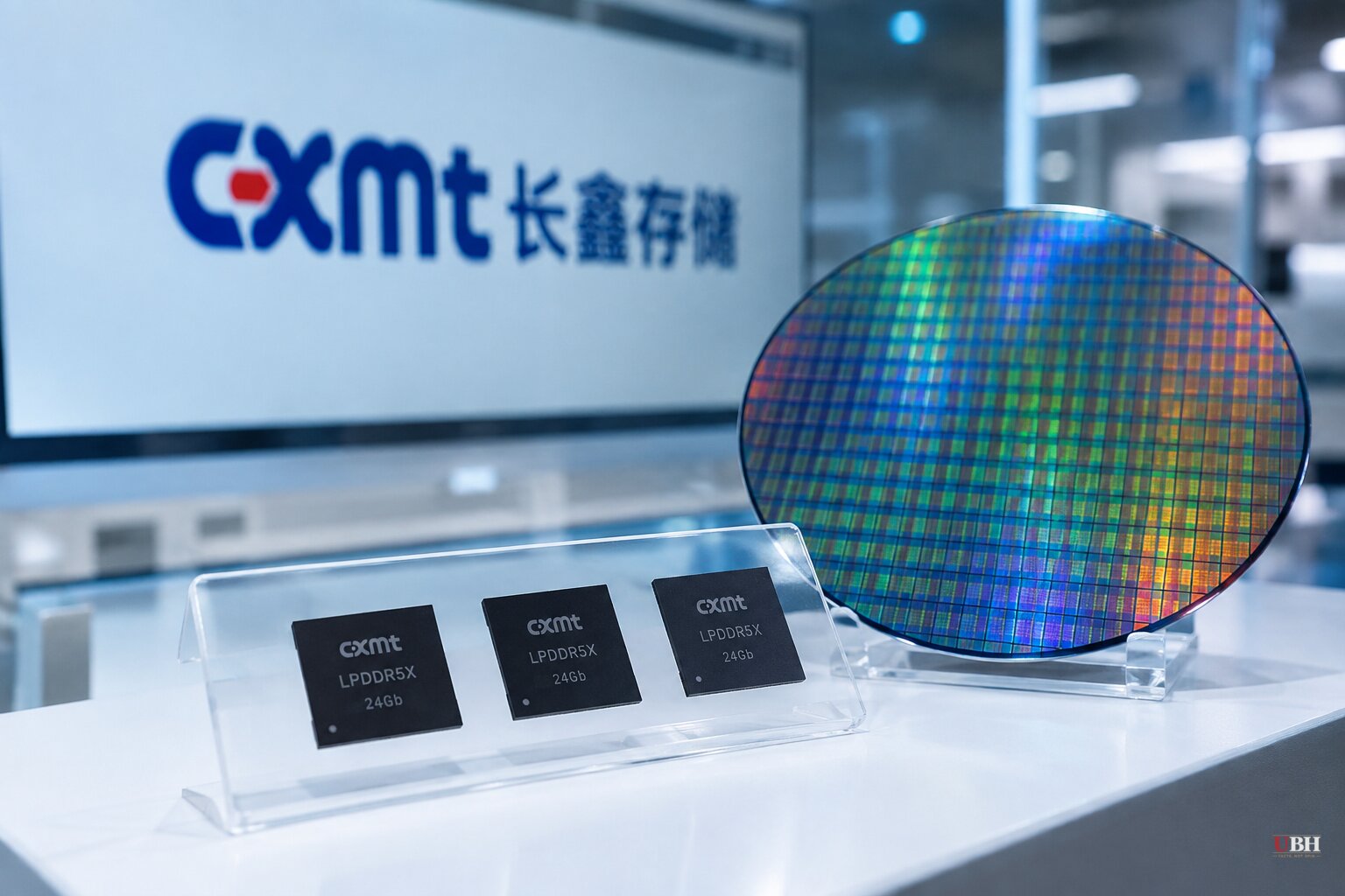
Since CXMT raised roughly $8.6 billion in its July 2026 IPO on Shanghai's STAR Market, the Hefei-based chipmaker has moved fast from capital raise to product launch. On Sunday, at the 2026 World Manufacturing Convention in Hefei, CXMT announced its fifth-generation, or G5, DRAM technology platform has entered mass production, according to Reuters and China Daily.
The headline products are two new 24-gigabit LPDDR5X memory chips, the low-power DRAM used in smartphones and portable electronics. Each holds 50% more data than CXMT's prior generation and comes in either a 496-ball or 245-ball package, the company said. Both are already in volume production, and China Daily reported the chips have "fully entered" mainstream domestic flagship smartphones, though CXMT vice president Luo Xiaodong did not name which handset makers are using them.
The technical claim, and why it matters
CXMT says it shrank the spacing of key data-storing structures to 11.95 nanometers using a technique it calls quadruple patterning, which repeats manufacturing steps to carve finer circuit patterns without the extreme ultraviolet lithography machines Washington has restricted China from buying. The company also cited a 45:1 capacitor aspect ratio and said the platform yields at least 50% more gross dies per wafer than its fourth generation, using an 8-gigabit baseline.
"Our process capability is now on par with the most advanced mass-produced nodes out there in the industry," Luo said, according to Reuters.
CXMT's claim of parity has not been confirmed by any independent lab, customer benchmark, or third-party teardown in these reports. Reuters itself frames the announcement as "a claimed breakthrough," and The News International noted the parity claim would only be significant "if proven true independently." Chinese chipmakers have a track record of announcing milestones at industry conferences that later prove more modest once outside engineers get their hands on the hardware.
Mezha.net's account of the same Reuters wire described the patterning technique as "triple patterning," while Reuters itself, China Daily, AsiaOne, The Business Times, and The News International all reported "quadruple patterning." That's a real discrepancy in the record. On the weight of five independent outlets citing the same term, quadruple patterning is the figure that holds up.
Scale is the bigger story than the nanometer number
CXMT's manufacturing scale is not in dispute. The company has grown from roughly 40,000 wafers per month in 2020 to about 300,000 wafers monthly across its Hefei and Beijing fabs today, according to Crypto Briefing, and is targeting 350,000 to 375,000 wafers per month by the end of 2026.
CXMT also disclosed a multi-year DRAM supply deal with Tencent worth roughly $3 billion, per Crypto Briefing, giving it a captive domestic customer as it scales. Combined with its STAR Market listing, CXMT now claims to be the world's fourth-largest DRAM supplier by market share and China's largest.
The export-control question nobody in these reports answers
Every outlet covering this story, from Reuters to The News International, frames CXMT's advance against the backdrop of U.S. export controls that have restricted China's access to advanced chipmaking equipment and software since 2022. None of the sources say whether Washington plans any new response to CXMT's announcement, and no U.S. agency statement appears in this coverage.
If CXMT's process claims hold up under independent scrutiny, it would suggest China's semiconductor industry is finding workarounds to lithography restrictions through repeated multi-patterning steps rather than needing the EUV machines Washington has blocked. If the claims don't hold up, it would suggest the restrictions are still doing meaningful damage to China's ability to match, not just approach, the industry's actual leading edge.
Samsung, SK Hynix, and Micron have not issued public responses to CXMT's Sunday announcement in any of the available reporting. Given CXMT's stated ambition to hit 375,000 wafers a month by year's end, the market will get a clearer read on whether the G5 platform's yields and reliability match the marketing within the next few quarters, once actual shipment volumes and any independent chip teardowns become available.
Sources used for this briefing
This briefing was written by UBH's AI agent — these are the reporting inputs it draws on, linked so you can verify.