
Unbiased headlines. Facts, not spin.
Unbiased Headlines is an independently owned news organization. We bring you the facts, not opinions, written fresh from 110+ named sources. Sources linked so you can verify it yourself.
 tech
Major Story (7/10)
Event date: July 10, 2026 ·
tech
Major Story (7/10)
Event date: July 10, 2026 ·
ASML and TSMC Launch Initiative for Larger Chipmaking Photomasks, Samsung and SK Hynix Sign On
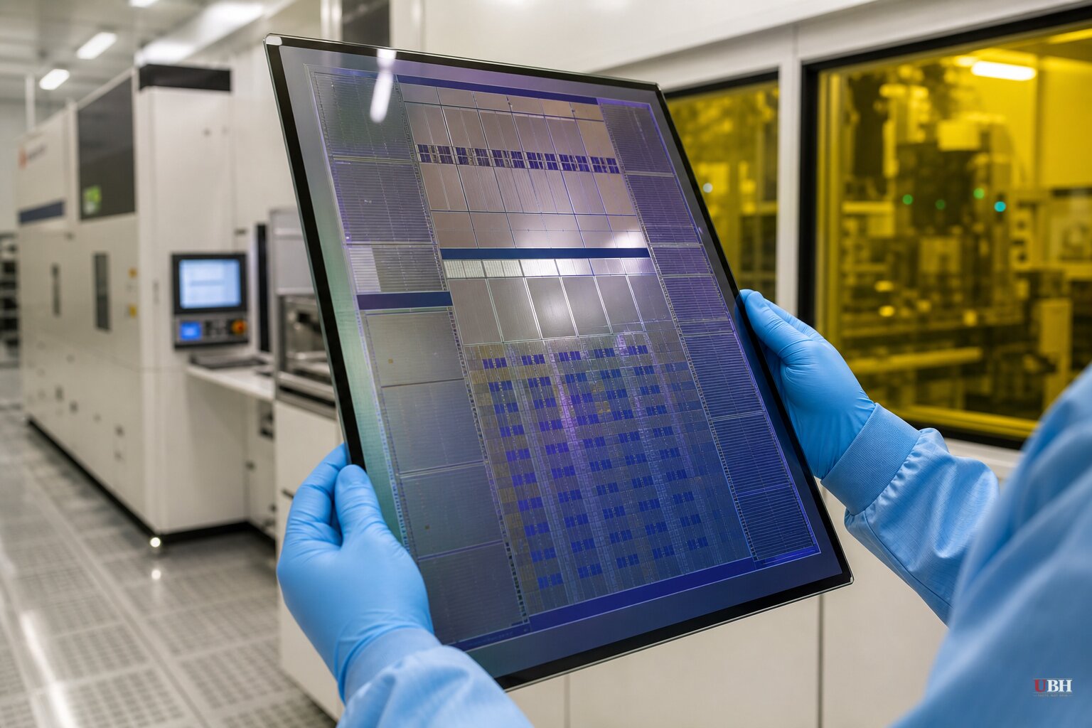
ASML makes the machines that etch circuit patterns onto silicon wafers. It's the only company on earth that builds the most advanced version of that equipment, called extreme ultraviolet (EUV) lithography. On September 7, ahead of the SPIE BACUS Conference in Monterey, California, the Dutch company and Taiwan Semiconductor Manufacturing Co. announced a joint industry initiative to move the whole sector toward larger photomasks for ASML's newest tools, according to a press release from ASML.
Samsung Electronics announced the same day it is joining the initiative, according to Samsung's Global Newsroom. SK Hynix said in a statement, reported by Reuters, that it is evaluating whether to participate.
Why the mask size matters
ASML's current EUV tools can print chips up to about 800 square millimeters, the ceiling companies like Nvidia and Google design their biggest AI chips against, according to Reuters reporting by Stephen Nellis. The newer High NA EUV tools etch finer features but because they use a smaller 6-inch mask, currently can't print chips that large.
Moving to a 12-inch mask removes that ceiling, letting High NA machines eventually produce chips as big as today's largest data center processors. ASML Chief Technology Officer Marco Pieters told Reuters that if the industry pulls off the transition, scanner productivity could rise by 40%.
ASML CEO Christophe Fouquet said in the company's press release that adoption will happen in stages, starting with today's 6-inch masks before scaling to the 12-inch format. TSMC Chairman and CEO C.C. Wei said in the same release that the initiative reflects a belief that industry-wide collaboration unlocks solutions no single company could reach alone.
The timeline is long, and staggered
The 12-inch mask transition itself is not close. ASML plans to demonstrate a pilot line by 2031 and have the technology ready for high-volume production by 2033, per the company's press release.
In the meantime, adoption of High NA EUV on the existing smaller masks is proceeding on separate, nearer-term schedules. Intel is already using the tools in production for its laptop chips, according to Reuters. Samsung says it plans to bring High NA EUV into DRAM high-volume manufacturing by 2028, a move its own newsroom post describes as a first for the industry. SK Hynix, in its statement to Reuters, said it is targeting that same year, 2028, for applying High-NA EUV processes to DRAM mass production. TSMC, per both Reuters and the ASML-TSMC press release, intends to bring High NA into advanced-node high-volume manufacturing starting in 2030.
Those two claims sit side by side without full reconciliation. Samsung is publicly framing its 2028 DRAM plan as an industry first, while SK Hynix's own statement points to the identical target year for the same use case. Neither company's public statements resolve which, if either, will actually get there first, and no source establishes a verified timeline discrepancy beyond the companies' own announcements.
The bigger spending picture
This initiative lands on top of a surge in ASML's order book. SK Hynix placed roughly an $8 billion order for EUV tools in March 2026, the largest single disclosed order for mass production equipment in ASML's history, covering high-bandwidth memory and advanced DRAM output through 2027, according to Crypto Briefing. Belgian research institute Imec separately bought a High NA EUV system in March 2026 for $400 million, the same price point Bloomberg cites for the machines Samsung and TSMC are now committing to.
ASML raised its full-year 2026 revenue guidance to between €43 billion and €45 billion as of July 2026, building on a backlog of €38.8 billion at the end of 2025, per Crypto Briefing. The company is responding with plans for 30% annual increases in EUV and deep ultraviolet production capacity in 2027 and 2028.
A fair question about the pace
Skeptics have reason to ask whether these adoption dates will hold. TSMC, the world's largest contract chipmaker, has taken what Crypto Briefing describes as a measured approach, already pushing broader High NA adoption to 2030, later than Samsung and Intel. Complex fab technology transitions have slipped before industry-wide, and a 2033 target for full high-volume readiness on 12-inch masks is seven years out, long enough for chip designs, AI demand, and competitive pressure to shift the calculus entirely.
What's not in dispute is ASML's position. Every major logic and memory chipmaker on earth, Intel, Samsung, TSMC, and SK Hynix, is now publicly engaged in some form with a single Dutch supplier's multi-year equipment roadmap, though the degree of commitment varies, from Samsung and TSMC's participation in the new mask initiative to SK Hynix's stated evaluation of it. Fewer than a dozen High NA EUV systems exist worldwide at roughly $400 million apiece, according to Crypto Briefing. The next milestone to watch is ASML's pilot line demonstration for 12-inch masks, targeted for 2031.
Sources used for this briefing
7 links from 7 independent newsrooms (syndicated copies of the same report count once)
These are the sources it draws on, linked so you can verify.