
Unbiased headlines. Facts, not spin.
Unbiased Headlines is an independently owned news organization. We bring you the facts, not opinions, written fresh from 110+ named sources. Sources linked so you can verify it yourself.
 tech
Notable (6/10)
tech
Notable (6/10)
ASML, TSMC and imec Report 94% Yield on 2D Material Transistors, a Step Beyond Silicon
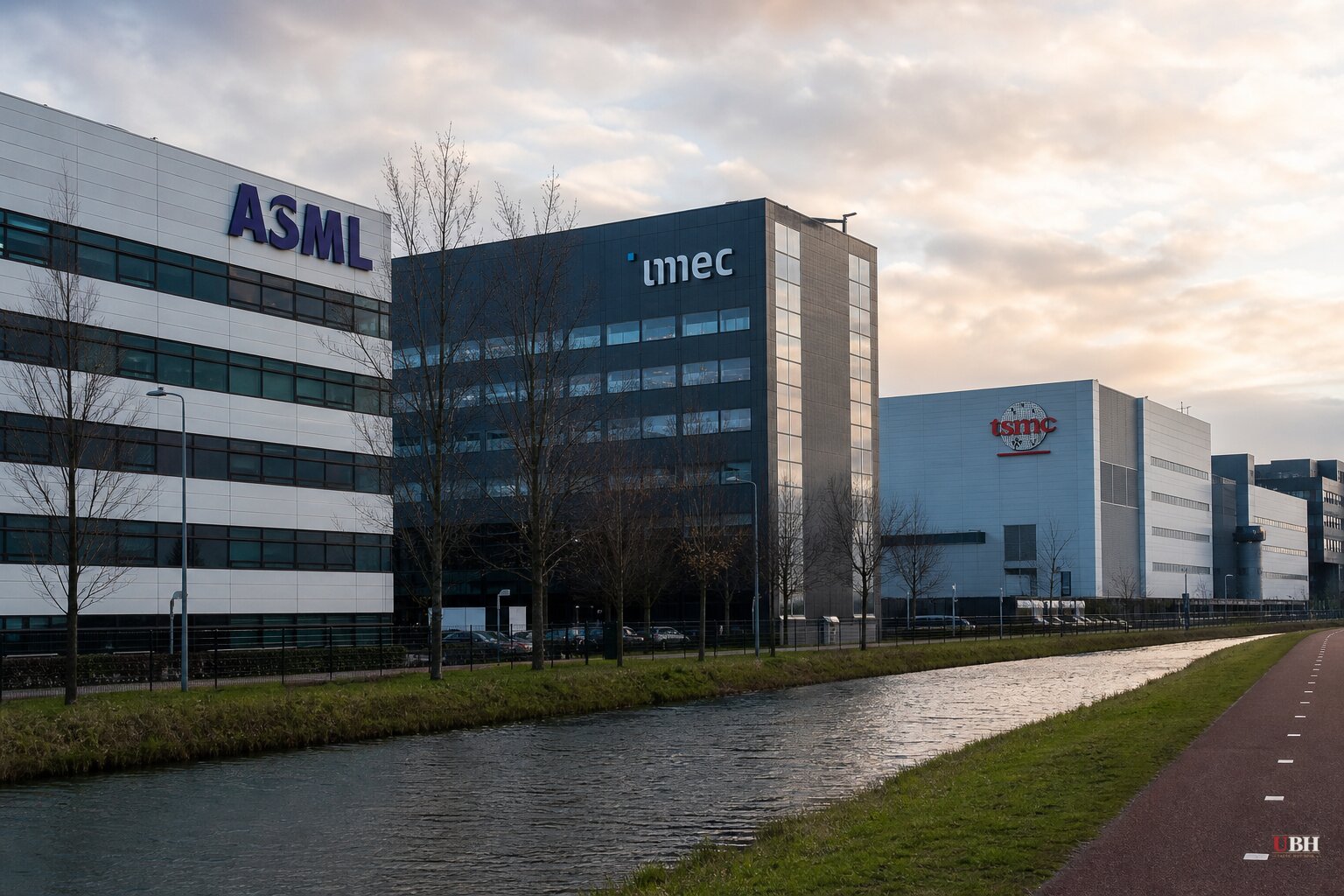
ASML, TSMC, and imec Report 94% Yield on 2D Material Transistors, a Step Beyond Silicon
Three of the semiconductor industry's biggest names just showed the clearest evidence yet that chips built from something other than silicon can actually work at scale.
ASML, TSMC, and Belgian research institute imec presented results in June 2026 at the IEEE/JSAP Symposium on VLSI Technology and Circuits, demonstrating what they describe as the first scaled complementary transistors built from two-dimensional materials on industry-standard manufacturing wafers. The headline number: a 94% yield rate, meaning nearly all the transistors on the wafer actually worked.
Lab demonstrations of exotic materials are common. Getting them to work reliably, at 94% success, on the exact 300mm wafers already used in commercial chip fabs, is a different proposition entirely.
What They Actually Built
The team produced both n-type and p-type transistors, the two building blocks needed for any modern logic chip, at a contacted poly pitch of 50 nanometers. Contacted poly pitch is the spacing between transistor gates. Smaller spacing means more transistors packed into the same silicon real estate.
The n-type devices used molybdenum disulfide, known as MoS2, as the channel material. The p-type devices used tungsten disulfide or tungsten diselenide. These are transition metal dichalcogenides, atomically thin crystal materials that can be laid down just a few atoms thick without the electrical leakage problems that plague silicon once you shrink it too far.
Both transistor types hit an Imax/Imin ratio exceeding 100,000, a measure of how cleanly the transistor switches between on and off, with very low off-currents at zero gate voltage. According to the companies, the tungsten diselenide p-type transistors performed near levels previously seen only in isolated lab settings, not in a repeatable manufacturing process.
Critically, all of it was fabricated using ASML's single-patterning extreme ultraviolet lithography, the same lithography technology already deployed in existing fabs. The team says the process is back-end compatible, meaning it could potentially slot into current chip manufacturing lines rather than requiring entirely new factories built from scratch.
Why Silicon Needed a Backup Plan
Silicon has carried the chip industry for six decades, but it is running into hard physics at the smallest scales. As transistors shrink toward single-digit nanometers, silicon channels start leaking current and losing the clean on/off switching that logic chips depend on. Two-dimensional materials sidestep that problem because they're inherently ultra-thin, without the same performance penalty.
The holdout has always been manufacturing, not physics. Growing these materials uniformly across a wafer, patterning them with precision, and integrating them into existing fab processes without wrecking their delicate atomic structure has been the challenge the industry kept facing. A 94% yield on a standard 300mm wafer suggests that challenge is beginning to crack.
TSMC's Vice President and Chief Technology Officer, Dr. Min Cao, called the collaboration pivotal in driving semiconductor innovation forward, framing the work around de-risking and speeding up the integration of new materials into actual production environments, according to Crypto Briefing's coverage of the announcement.
What Still Isn't Known
None of the companies involved put a date on when 2D material transistors show up in a phone, laptop, or data center chip. A conference demonstration, even a strong one, is not a product roadmap. Yield on a research wafer with a handful of test devices is also a different challenge than yield across billions of transistors on a commercial logic chip running at full clock speed for years.
The stakes behind this go beyond lab results. TSMC is the backbone of Taiwan's chip industry and the primary manufacturer for Apple, Nvidia, and AMD. ASML, based in the Netherlands, is the sole supplier of the extreme ultraviolet lithography machines that make advanced chipmaking possible anywhere in the world. Both companies sit at the center of Western efforts to keep advanced semiconductor manufacturing out of Chinese hands, and any technology that extends the life of that manufacturing edge carries weight well beyond the lab bench.
The next test is whether this scales from a demonstration wafer to a repeatable manufacturing process imec, ASML, and TSMC are willing to commit real fab capacity to. Neither company has set a timeline for that decision.
Sources used for this briefing
1 link from 1 independent newsroom (syndicated copies of the same report count once)
These are the sources it draws on, linked so you can verify.