
Unbiased headlines. Facts, not spin.
Unbiased Headlines is an independently owned news organization. We bring you the facts, not opinions, written fresh from 110+ named sources. Sources linked so you can verify it yourself.
 tech
Notable (6/10)
Samsung to Build Nvidia NVHBM Base Dies on TSMC's 3nm Process, Seoul Economic Daily Reports
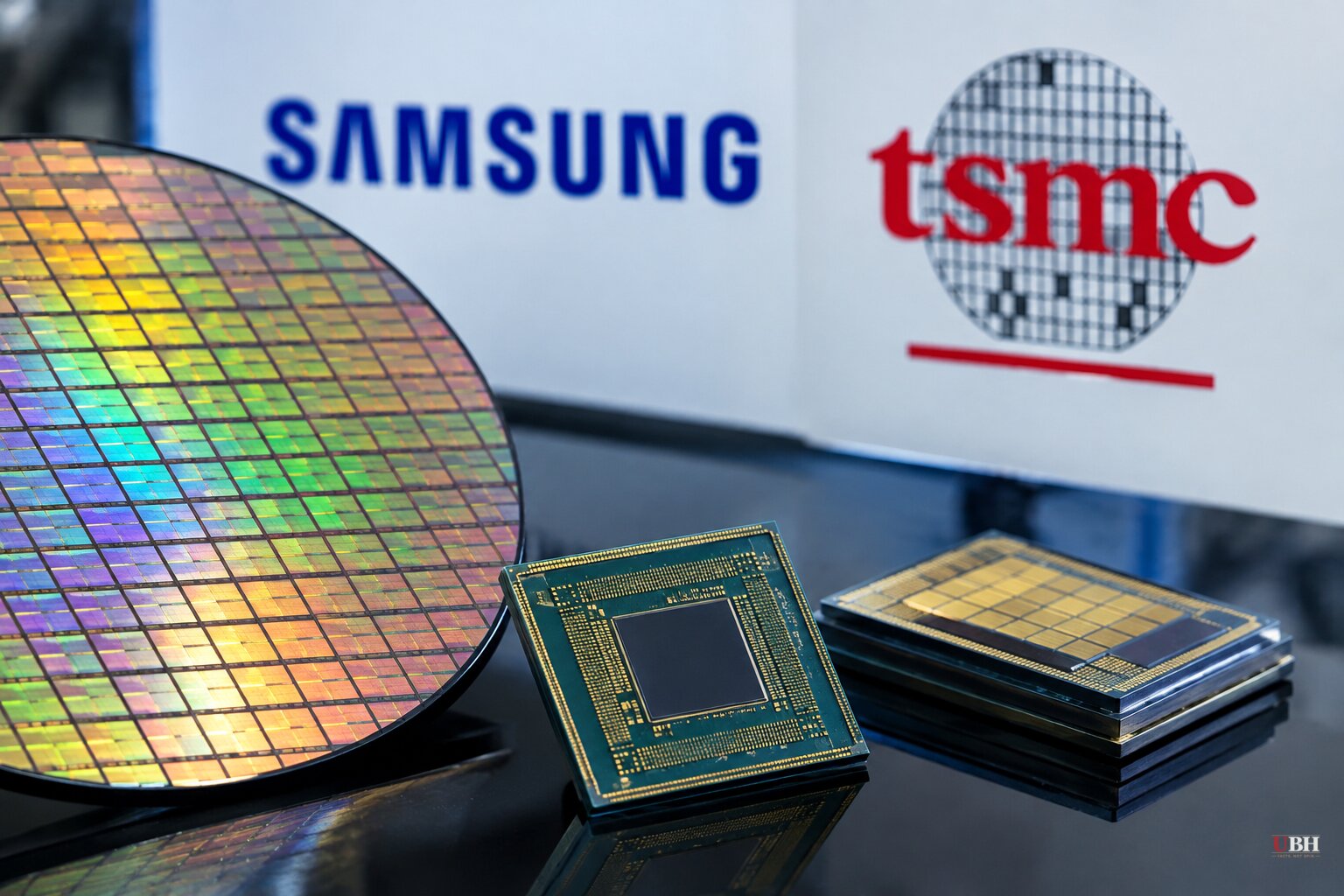
Since Nvidia unveiled its NVHBM custom memory design on Aug. 26, the open question has been who would manufacture the logic chip at the bottom of each stack. Seoul Economic Daily reported Sunday, Oct. 18, that Samsung Electronics will make that chip on TSMC's 3nm process, not on its own foundry lines.
The report rests on unnamed industry sources. It says the decision followed an internal review by Samsung's Device Solutions division, which runs the foundry business.
What Nvidia asked for
According to the report, Nvidia asked all three of its high-bandwidth memory suppliers (Samsung, SK Hynix and Micron Technology) to build NVHBM base dies on TSMC's 3nm process. Nvidia also wants the core DRAM dies on the sixth-generation 1c process.
The reasoning, as relayed in the report, is consistency. If each supplier uses different manufacturing methods, the designed performance is harder to reproduce and Nvidia has to validate each vendor's product separately.
SK Hynix and Micron already source base dies from TSMC's 3nm process, according to the report. Samsung is the last of the three to line up.
Why the base die suddenly matters
The base die sits at the bottom of the memory stack. In earlier HBM generations it was mostly a passive routing layer, and the memory controller lived on the GPU.
NVHBM moves that controller into the base die. Nvidia says the design delivers up to 30% more memory bandwidth, 15% lower HBM power use and 25% more compute die area on the accelerator, all measured against standard HBM4E. The physical layer was shrunk by 60% to make room for the controller.
Packing that logic into a memory base die calls for an advanced logic process, which is where the foundries come in.
The yield gap
Industry estimates put TSMC's 3nm yield above 90%. The same estimates put Samsung Foundry's comparable 2nm SF2 process at roughly 60%. One outlet, Tech Times, cites a range of 50% to 60% for SF2 and describes the gap as disqualifying for Samsung at the top of the AI memory market.
Those are estimates, not figures published by either company. Neither TSMC nor Samsung has disclosed yield data for these processes.
The Seoul Economic Daily account frames Samsung's decision as acceptance of Nvidia's requirements after review. It does not say Samsung concluded its own process had failed.
Capacity is the other pressure
Supply is tight. UBS projects HBM demand next year at about 61.5 billion gigabits, up 91% from this year, against new shipments of about 54.6 billion gigabits. That leaves a shortfall of roughly 10% to 11%.
Samsung's own base die capacity is limited to Hwaseong Line 17 and part of its Pyeongtaek P3 line. Turning to TSMC adds capacity without waiting for new fabs.
TSMC is not unconstrained either. On its Oct. 15 earnings call it flagged tight 3nm capacity, with the node making up 33% of third-quarter wafer sales, its largest share of any node. According to Economic Daily News, Chairman and CEO C.C. Wei announced another 3nm fab in Tainan, set for mass production in the first half of 2028. That comes on top of expansion in Arizona, Kumamoto in Japan and the Southern Taiwan Science Park.
What Samsung keeps
Samsung is not giving up its integrated model across the board. For standard HBM it will keep making base dies on its own 4nm process. That covers HBM4, which entered mass production earlier this year, and HBM4E, which is in production validation. Core dies for both come from 1c lines at Hwaseong and Pyeongtaek.
Samsung also plans to stay with its in-house approach for custom HBM sold to other customers such as AMD. According to the report, it is validating NVHBM base die production on its own 2nm process in case demand outruns TSMC's capacity.
The two companies have worked together before. Samsung and TSMC first collaborated four years ago on making HBM compatible with TSMC's GPU packaging. This would be the first time they cooperate at the HBM manufacturing stage.
Two readings of the deal
Tech Times calls it a striking collapse of the vertical integration model Samsung's memory division has relied on for decades. It says TSMC would become the sole logic manufacturing partner for every premium AI memory program on Nvidia's roadmap.
Gokhshtein Media reads it differently. It says the dual-track approach suggests Samsung views the outsourcing as temporary leverage, not a permanent exit.
Both readings agree on one fact. Nvidia, as the largest HBM buyer, is setting component standards for its suppliers, and the foundry behind those standards is TSMC.
The concentration is concrete: three memory makers, one logic foundry. Samsung competes with TSMC for customers including Qualcomm and Tesla, yet would now depend on it for the most complex part of its flagship Nvidia memory product.
What to watch
Samsung has not publicly detailed volumes or timing for NVHBM base dies. The test is whether TSMC's 3nm lines can absorb three memory makers' demand alongside AI accelerators and smartphone chips, and whether Samsung's 2nm validation reaches a point where it can actually take on that overflow.
Sources used for this briefing
7 links from 7 independent newsrooms (syndicated copies of the same report count once)
These are the sources it draws on, linked so you can verify.